Technologists from GLOBALFOUNDRIES and Nikon Report on Computational Lithography Solutions in Manufacturing
In a LithoVision presentation entitled “SMO Application for 28 nm Metal Patterning at GLOBALFOUNDRIES using the S620D” Rolf Seltmann, GLOBALFOUNDRIES Fellow, explained the importance of vendor-to-vendor scanner matching and presented source mask optimization (SMO) results demonstrating marked improvements to process window and other metrics. Tomoyuki Matsuyama, Nikon Strategic Imaging Solutions Section Manager, delivered a complementary presentation describing Nikon computational lithography solutions for SMO, scanner matching, and post-mask optimization.
In Seltmann’s introduction he explained that the 28 nm node is one of the last nodes where single patterning can be utilized, but it has a very limited process margin. Like many other chip manufacturers, GLOBALFOUNDRIES has a dual-supplier strategy for their immersion scanners. With this strategy, if a chipmaker does not want to dedicate particular layers to a single vendor, excellent matching between tool platforms from different vendors is critical. Both overlay and optical-proximity effects (OPE) must be matched. In particular, OPE matching removes the need for vendor-specific OPC models. The need for specialized illumination sources via source mask optimization and the ability to match one vendor’s solution on another vendor’s scanner were the focus of Seltmann’s insightful LithoVision presentation.
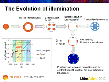
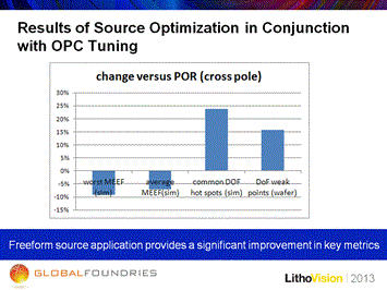
Reminding the audience that 28 nm node lithography does not benefit from wavelength or numerical aperture jumps, Seltmann said new computational lithography solutions are necessary. He described the evolution of illumination and the transition from conventional to annular sources for better resolution, followed by quadrupole for enhanced line/space contrast, and onward. He explained that while freeform illumination does not provide inherent resolution and/or contrast improvements, it is an “enabler” for computational lithography (figure 1A). For an example layer at their 28 nm node, pitch restriction was not allowed, making it necessary to investigate how well the printability of the features could be improved with a freeform source. The results obtained using source optimization in conjunction with OPC tuning were very encouraging. Seltmann reported that when freeform source application was compared to the cross pole process of record (POR), there was a significant improvement in the key metrics including mask error enhancement factor (MEEF) and depth of focus (DOF) (figure 1B).
Figure 1A. Seltmann described the evolution of scanner illumination (left image). Figure 1B. When freeform source application was compared to the cross pole POR, there was a significant improvement in key performance metrics.
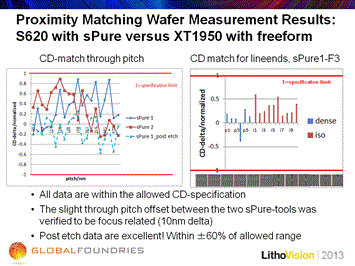
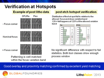
Seltmann explained that since the GLOBALFOUNDRIES S620D immersion scanners were not configured with freeform illuminators, they investigated matching capabilities for 28 nm metal patterning using Nikon sPURE optics designed to match the freeform source solution. He stated that Nikon demonstrated an excellent intensity match between a freeform target source and a specially designed sPURE. A simulated CD response study comparing sPURE vs. freeform systems confirmed that the two sPURE systems fit well into the distribution of the systems with the freeform illuminators. It also showed the matching between an sPURE and a freeform system can be as good as between two freeform systems. Seltmann reported that proximity matching results between an S620D using sPUREs and an competitor NXT1950 system with freeform illumination showed all CD data within specification and that post-etch data was excellent, staying within ±60% of the allowed range (figure 2A). In addition, post-litho data verified that S620D sPURE and NXT1950 freeform patterning was well matched within the focus variation band. Finally, post-etch hotspot verification showed no significant difference in fail statistics─with both tool classes having sufficient process window (figure 2B).
Seltmann concluded that pixelated sources are a key enabler for computational lithography, and that Nikon has demonstrated excellent CD matching between a non-Nikon freeform source target and a specially designed Nikon S620D freeform sPURE, and noted his anticipation for the Nikon Intelligent Illuminator capabilities.
Figure 2A. Proximity matching results between an S620D using sPUREs and an NXT1950 system with freeform illumination showed all data within the allowed CD-specification and post etch data was excellent (left image). Figure 2B. Good overlay and proximity matching were also confirmed by yield matching.
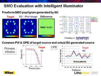
Matsuyama’s complementary LithoVision presentation on “Computational Lithography in Practice” discussed how Nikon supports computational lithography through numerous key areas, including freeform illumination and OPE matching. He explained that the newly released S622D includes the Nikon Intelligent Illuminator Unit (IIU), a freeform illumination source. He explained that the iPURE unit, which is the optical engine of the Intelligent Illluminator, can generate pupilgrams to match essentially any customer request. Matsuyama reported that SMO evaluations using the Intelligent Illuminator confirmed that the process window and OPE of features simulated with the actual Intelligent Illuminator generated source are well matched with those from the target source (figure 3A).
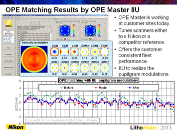
Figure 3A. Process window and OPE of features simulated with the actual Intelligent Illuminator generated source are well matched with those from the target source (left image). Figure 3B. CD differences were significantly improved using OPE Master for the S621D with IIU modulations. CD matching errors were reduced from ~1.5 nm to 0.75 nm (RMS) and matched the predicted OPE well.
Nikon also supports computational lithography through OPE matching, and Matsuyama explained how OPE Master interacts with the Intelligent Illuminator. OPE Master accepts CD data from the scanner of interest and from a reference, and then recommends IIU adjustments to minimize the difference between them. He noted that it is possible to do Nikon to Nikon matching and Nikon to Non-Nikon matching (as GLOBALFOUNDRIES did above). OPE matching studies have shown that CD differences were significantly improved using OPE Master for the S621D with IIU modulations. CD matching errors were reduced from ~1.5 nm to 0.75 nm (RMS) and matched the predicted OPE well (figure 3B).
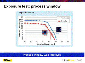
Matsuyama then described how after the mask is made there is still room for optimization to avoid performance limitations due to mask errors or other effects. He announced that a new Nikon software tool recovers performance using IIU pupilgram freedom and can optimize for process window, MEEF, and OPE with IIU-aware optimization available. As shown in lithographic measurements (not simulation), this Source Global Optimization software has successfully improved the S621D immersion scanner process window without impacting OPE behavior (figure 4A).
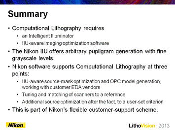
Matsuyama concluded his detailed presentation by stating that advanced computational lithography requires an Intelligent Illuminator with IIU-aware imaging optimization software, and that Nikon software supports numerous computational lithography solutions as part of a flexible customer support scheme to enable next-generation manufacturing (figure 4B).
Figure 4A. Source Global Optimization software successfully improved the S621D immersion scanner process window without impacting OPE behavior (left image). Figure 4B. Nikon software supports numerous computational lithography solutions as part of a flexible customer support scheme to enable next-generation manufacturing.
