Intel and Nikon Litho Specialists Discuss Overlay Matching and Edge Placement Error for Production Beyond 20 nm
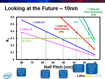
Sam Sivakumar, Intel Corporation Fellow and Director of Lithography, reported at LithoVision that the biggest challenges to next-generation lithography are edge placement error (EPE) and management of multiple exposure passes per layer. Nikon specialists also discussed how advancements in scanner mix-and-match overlay, focus, and CD control are enabling ArF immersion to support sub-20 nm half-pitch processes. Sivakumar’s detailed presentation, entitled “Enabling Production Beyond 20 nm,” began with an update on the Intel roadmap, which includes single-pass 193 nm immersion lithography (193i) at the 22 nm node, pitch halving with multiple-pass 193i lithography for the 14 nm node in 2013, and 193i pitch quartering - potentially combined with EUV lithography, for the 10 nm node in 2015 (figure 1A).
Sivakumar explained that a key challenge in printing at these nodes is that while 1-dimensional structures scale well, 2-dimensional structures do not. Thus, lithography of 2-D features at these nodes requires two operations: printing of a basic underlying grating followed by printing of cuts to form 2-D features. These present fundamentally different challenges to both the designer and the lithographer. The design aspect is seen in comparing a 65 nm layout with a 45 nm layout. At 65 nm there were bidirectional features, with varied gate dimensions and pitches, whereas at 45 nm there are unidirectional features, uniform gate dimension and a gridded layout. Gridded architectures are now standard.
Fortunately, ArF extension can deliver the necessary grating pitches for the foreseeable future with spacer-based pitch halving (P/2), followed by spacer-based pitch quartering (P/4), and potentially on to P/6 and P/8 techniques.
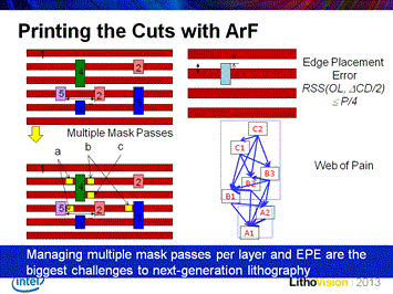
Figure 1A. Sivakumar shared a view of the Intel technology roadmap (left image). Figure 1B. When printing the cuts with ArF, Sivakumar reported that edge placement error and management of multiple exposure passes per layer are the biggest challenges to next-generation lithography.
As for printing the cuts, Sivakumar reported that edge placement error and management of multiple exposure passes per layer are the biggest challenges to next-generation lithography, and reminded the audience of the associated multilayer “web of pain” from coordination of the multiple passes on different tools (figure 1B). He contrasted this with EUV, which can simplify cutting and hole patterning using fewer mask passes. He concluded that ArF pitch division is the most likely scenario for printing the gratings, whereas the final patterning technique for the cuts and vias will depend upon technology development and cost of ownership over the next two years.
Sivakumar proceeded to explain the key sources of EPE. These include intrinsic lithography overlay/CD control on the scanner in the presence of wafer non-ideality, etch interactions with associated feature size/pitch dependencies, optical proximity correction (OPC), and thin film deposition variability. Therefore, key focus areas should include intrinsic tool performance improvements, thorough characterization of through-pitch and feature-size dependent etch interaction, as well as a heavy dependence on computational lithography in order to minimize error. Accurate through-pitch modeling is essential for minimizing EPE error – with litho variation, etch variation, and post treatments including resist hardening, CD reduction, and linewidth roughness (LWR) mitigation all being critical. He explained that both linewidth and line-end effects must be accounted for and that cooperation between the lithographers and the etch engineers is essential.
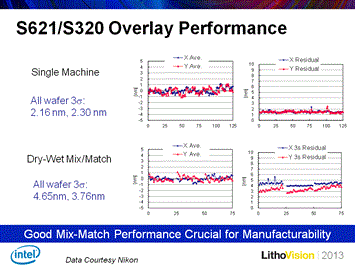
In reviewing current Nikon performance, Sivakumar stressed that good scanner mix-and-match performance is crucial for manufacturability (figure 2A). He reported that S621D immersion to S320F dry ArF overlay matching has exhibited excellent results with 3σ data improved from x=9.4, y=6.0 nm to x=3.8, y=3.3 nm after field matching correction. In addition, 3σ mix-and-match overlay (MMO) data across 3 lots was < 5 nm for all wafers.
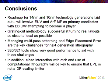
Figure 2A. Sivakumar reminded the audience that good scanner mix-and-match performance is crucial for manufacturability (left image). Figure 2B. Sivakumar concluded that the roadmap for 14 nm and 10 nm technology generations are laid out and will involve EUV and ArF multiple patterning as the primary candidates.
In closing, Sivakumar stated that the roadmap for 14 nm and 10 nm technology generations are laid out and will involve EUV and ArF multiple patterning as the primary candidates, with ebeam direct write lithography attempting to become a player (figure 2B). While the grating/cut method is effective in producing real layouts as close to ideal as possible, managing multi-pass patterning and edge placement error are the key challenges for next-generation lithography, and close interaction with etch and the use of computational lithography will be vital to ensure EPE does not limit design rule scaling. He announced that the S320F and S621D tools have demonstrated very good performance to aid with these challenges.
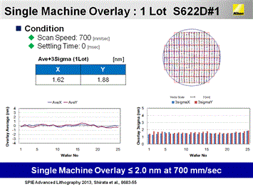
In complementary presentations at LithoVision and SPIE Advanced Lithography, Ryoichi Kawaguchi, Nikon System Development Engineer, and Yosuke Shirata, Nikon Development Engineer, provided updates on current immersion performance. Kawaguchi reported that overlay, focus, and CD control are critical to current and future lithography. Starting with the current tool, the S621D, he showed machine-to-machine overlay (MMO) data across the lot below 4.2 nm (Avg. + 3σ), as well as focus uniformity data, measured by a phase shift focus monitor (PSFM), including edge shots, of 12.8 nm (3σ). Recognizing that further enhancements in scanner mix-and-match overlay, focus, and CD control are essential for sub-20 nm applications, he offered an overview of the many improvements provided by the newly released NSR-S622D immersion scanner. These S622D advancements were discussed in detail by Shirata. Based on the well-known Streamlign platform, the S622 utilizes the proven Bird’s Eye Control system combined with an enhanced reference grating plate; this increases stability, and reduces the need for calibrations, boosting productivity. Reticle expansion effects are mitigated using a Reticle Cooling System that minimizes thermal deformation of the reticle, while a Wafer Table Temperature Control System using a feedback loop is employed to optimize temperature stability and grid distortion during exposure to further improve overlay. Shirata reported that together these comprehensive systems enable the S622D to deliver single machine overlay (SMO) less than 2 nm. The S622D has demonstrated SMO 3σ potential of 0.7 nm, as well as SMO (Avg. + 3σ) x=1.6 nm, y=1.9 nm across the lot (figure 3A), and SMO stability below 2.5 nm has been maintained across 5 days.
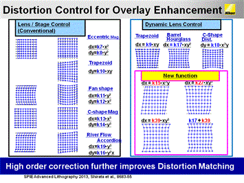
Figure 3A. The S622D has demonstrated single machine overlay stability across the lot below 2 nm (Avg. + 3σ) (left image). Figure 3B. The S622D Dynamic Matching Adjustment Control system compensates for high-order distortion signatures (trapezoid, keystone, etc.) to optimize MMO performance and manufacturing flexibility.
He also described how enhancements to lens performance, autofocus, and other system advancements enable S622D MMO to reach and go below 3.5 nm. The S622D autofocus system minimizes process-dependent effects with an improved optical design, and edge focus accuracy has been tightened by a new sensor layout to aid yield enhancement at the wafer edge. He reported that PSFM across wafer focus control of 11 nm (including edge shots) has been achieved, and a focus stability range of 9.1 nm was maintained across a one week period. In addition, autofocus sensor error of less than 2 nm for various product wafers was shown. He explained that S622D lens distortion was also reduced by almost 40% compared to the previous generation scanner, with dynamic distortion single machine and matching results both less than or equal to 1.5 nm (3σ).
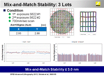
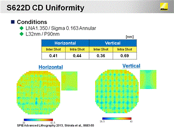
This is combined with further developments in the compensation functions that adjust the grid and distortion of one scanner to another. Shirata stated that while a number of dynamic lens control functions were already available, the S622D Dynamic Matching Adjustment Control system now also compensates for high-order distortion signatures (trapezoid, keystone, etc.) to optimize mix-and-match overlay performance and manufacturing flexibility (figure 3B). He reported that MMO using two S622D tools showed total overlay error across 3 lots below 3 nm (Avg. + 3σ) (figure 4A). Shirata also noted that these numerous system enhancements, paired with advanced aberration control solutions enable the S622D to deliver ultra-fine CD uniformity control for sub-20 nm processes (figure 4B).
Figure 4A. The S622D has demonstrated MMO (Avg. + 3σ) below 3 nm across multiple lots (left image). Figure 4B. The S622D delivers ultra-fine CD uniformity control for sub-20 nm processes.
In Kawaguchi’s LithoVision wrap-up, he announced that ArF extension will continue and ArF immersion will support sub-20 nm half-pitch imaging processes through ongoing extension of the S622D Streamlign platform and further enhancements to overlay and CD uniformity. Finally, in an industry first, Nikon will also apply this platform to 450 mm wafer production.
