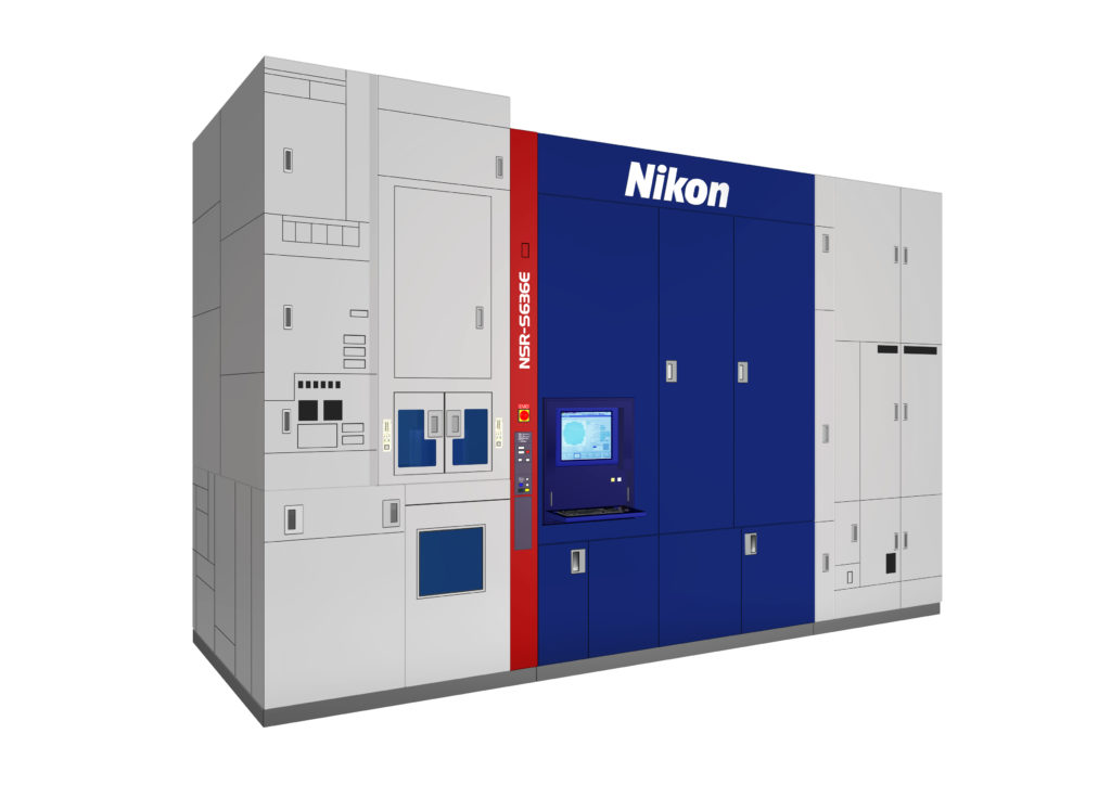
Tokyo, Japan – October 18, 2021 – Nikon Corporation (Nikon) announced it is currently developing the next-generation NSR-S636E ArF immersion scanner, which will deliver superior overlay accuracy and ultra-high throughput to support manufacturing of the most critical semiconductor devices. Product sales are scheduled to begin in 2023.
As the digital transformation (DX) accelerates, there is an essential need to process and communicate tremendous volumes of data very quickly. High-performance semiconductors are imperative to satisfy these requirements, and semiconductor device technology is progressing with a simultaneous focus on circuit pattern miniaturization as well as 3-dimensional (3D) device structure development.
The NSR-S636E features an enhanced inline Alignment Station, or iAS, which is a wafer pre-measurement module integrated between the coater/developer unit and the lithography scanner. The S636E and iAS utilize sophisticated multi-point alignment measurement and high order correction functions that enable device makers to achieve the stringent overlay accuracy necessary for 3D device structures, while also maximizing immersion scanner productivity. The NSR-S636E is well-suited for cutting-edge semiconductor manufacturing including logic and memory devices, CMOS image sensor applications and more.
Nikon is committed to providing industry-leading lithography solutions like the NSR-S636E immersion scanner that enable customers to advance semiconductor manufacturing and help drive the digital transformation.

The information contained in this press release is current as of its date of publication.
About Nikon
Since 1980, Nikon Corporation has been revolutionizing lithography with innovative products and technologies. The company is a worldwide leader in semiconductor lithography systems for the microelectronics manufacturing industry with more than 8,000 (semiconductor) lithography systems installed worldwide. Nikon offers the most extensive selection of production-class steppers and scanners in the industry. These products serve the semiconductor, flat panel display (FPD) and thin-film magnetic head (TFH) industries. Nikon Precision Inc. provides service, training, applications and technical support, as well as sales and marketing for Nikon lithography equipment in North America. For more information about Nikon, access our website at https://www.nikonprecision.com.
####
This press release contains forward-looking statements as that term is defined in the Private Securities Reform Act of 1995, which are subject to known and unknown risks and uncertainties that could cause actual results to differ materially from those expressed or implied by such statements. Such statements are subject to risks, uncertainties and changes in condition, particularly those related to industry requirements and other risks. The Company undertakes no obligation to update the information in this press release.
For further information, contact:
Holly Magoon, Senior Marketing Manager
Nikon Precision Inc.
holly.magoon@nikon.com
