DNP and AZ-EM Speakers Identify the Need for Lithography Paradigm Changes
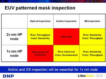
At the recent LithoVision symposium, Dai Nippon Printing Fellow Naoya Hayashi provided an update on “Mask Challenges and Solutions for Next Generation Lithography” and described a paradigm shift in NGL solutions. He reported that while optical extension with multiple patterning is admittedly complex and costly, EUVL requires complex masks, scanners, and dedicated infrastructure. Challenges in mask inspection were one example. Inspection can be performed at either optical wavelengths or at the actinic 13.5 nm wavelength. Optical inspection should suffice for the 2x nm node, but will not have the resolution needed for the 1x nm node. Conversely, actinic inspection is not ready now, but will be required for the 1x nm node and beyond (figure 1A). Hayashi discussed some of the infrastructure development that is underway to meet these needs.
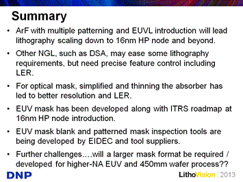
On the 193 nm extension topic, Hayashi believes that 193i lithography with multiple patterning and EUV introduction will enable lithography scaling to 16 nm and beyond. Optical masks also face challenges, in that they will need new smaller sub-resolution features and tighter CD uniformity. One sign of progress is that simplifying and thinning absorbers for optical masks have led to better resolution and improved line-edge roughness (LER); for instance, new blank and coating materials are expected to show a 20% line-edge roughness improvement. Hayashi also pointed out that the industry needs to reach consensus on whether a larger 9-inch mask will be required for higher-NA EUV and 450 mm wafer processing in the future. Looking forward to next-generation lithography candidates (other than EUV) Hayashi noted that while precise line-edge control will still be needed for any type of hybrid or complementary lithography, directed self-assembly (DSA) shows promise in that it could relax the requirements for critical processes (figure 1B).
Figure 1A. Hayashi reported that optical inspection should suffice for the 2x nm node, but will not have the resolution needed for the 1x nm node. Conversely, actinic inspection is not ready now, but will be required for the 1x nm node and beyond (left image). Figure 1B. Hayashi noted that the industry needs to reach consensus on whether a larger 9-inch mask will be required for higher-NA EUV and 450 mm wafer processing in the future.
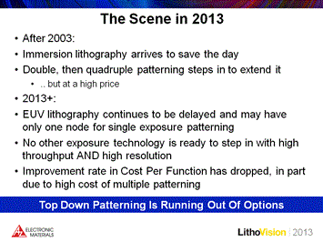
This was followed by a presentation from Dr. Ralph Dammel, AZ Electronic Materials Chief Technology Officer, who warned the audience that top-down patterning is running out of options. His insightful presentation entitled “Directed Self-Assembly: Changing the Lithography Paradigm” focused on the need for an industry paradigm shift towards bottom-up lithography using smarter materials. Dammel began his visionary talk with a comparison of 2003 conditions to 2013. He noted that, in both cases, EUV implementation was predicted within a few years, and likened directed self-assembly’s current state to how immersion lithography was just taking off in 2003. He then provided a more detailed view of the industry scene in 2013—explaining that continued EUV delays could limit its usage to only one node for single exposure patterning, and highlighting that there isn’t another exposure technology ready to deliver high throughput with the necessary resolution. In addition, the improvement rate in cost per function has declined, partially due to the added cost of multiple patterning. Dammel referenced Qualcomm data from SPIE Advanced Lithography 2012, which showed that while in the past eight years relative cost per gate has decreased by ~29%/year, the cost reduction starts to level off at 20 nm due to EUV cost/timing and multiple patterning cost issues. These factors led him to conclude that top-down patterning is running out of options (figure 2A).
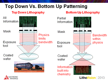
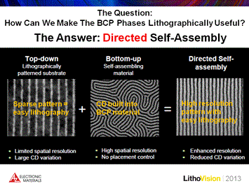
Figure 2A. Various factors led Dammel to conclude that top-down patterning is running out of options (left image). Figure 2B. Dammel explained the key differences between the industry’s current top-down lithography and his vision of bottom-up lithography.
Dammel described how the industry has been able to cheat “Tennant’s Law,” which relates throughput in pixels/sec to resolution in nm, for quite some time through wavelength transitions and scanner improvements, etc., but cautioned that we are running out of physics solutions to continue on this path. He proposed that instead of being able to simultaneously have smaller, cheaper, and faster technology, it will be necessary to pick only two of those components, unless there is a change to the industry paradigm. Dammel believes smarter materials are a viable solution for this challenge. He contrasted the key differences between the industry’s current top-down lithography model, wherein physics limits the bandwidth and there is a heavy reliance on scanner technology, with his vision of bottom-up lithography, where the imaging is held within the limits of physics and the additional information is built into the chemistry (figure 2B).
This led to a discussion of the basics of directed self-assembly (DSA) with block copolymers (BCP). Dammel explained that it is possible to control the type of monomers, the overall length (molecular weight), and the relative length (molar fraction fA) of block copolymers, and that the phase diagram of the BCPs depends upon the molecular weight (number of molecules N) and strength of interaction described by a χ factor. Within the phase diagram for two-component block copolymers, multiple structures are available, including cylindrical and lamellar phase structures. Cylindrical phase structures resemble lithographic contact holes, and lamellar phase structures actually look similar to lithographic line and space structures. By themselves, the different BCP phases are not useful as they orient randomly, but due to these unique characteristics, the BCP phases can be made useful with directed self-assembly, creating high-resolution patterns utilizing relatively simple lithography (figure 3A). Two methods exist: graphoepitaxy, which uses physical patterns like lines and spaces to constrain the BCP, and chemoepitaxy, which uses chemical areas on the wafer to do the same.
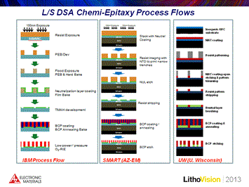
Figure 3A. Dammel explained that BCP phases can be made useful with directed self-assembly, creating high-resolution patterns utilizing relatively simple lithography (left image). Figure 3B. Comparison of viable line/space DSA chemiexpitaxy process flows.
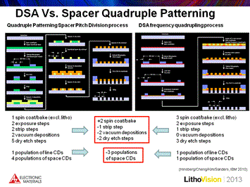
Dammel gave an example of an IBM process flow for line/space DSA and noted how the litho-friendly 193 nm exposure process used standard solvents, was track compatible, and each step required less than 2 minutes. An IBM process flow based on 193 nm dry lithography with a 150 nm pitch dry resist pattern that used 6x pitch frequency multiplication to generate a 12.5 nm (1:1) DSA pattern was also shown, along with a comparison of viable line/space DSA chemiepitaxy process flows from IBM, the University of Wisconsin, and the SMART process by AZ Electronic Materials (figure 3B). When a DSA frequency quadrupling process was compared to a quadruple patterning spacer division process, it was noted that although the DSA process would add 2 spin coat/bake steps, the other process steps were all reduced and there were also three fewer populations of space CDs helping to reduce the inherent overlay errors (figure 4A).
DSA can be used for both frequency multiplication (as mentioned above) and contact hole (CH) rectification. It is believed that chemiexpitaxy will mostly be used for frequency multiplication in line/space patterns, with contact holes employing both chemi- and graphoepitaxy solutions. In the case of CH rectification, graphoepitaxy will be used for CDU improvement and CD shrink. Dammel reported that AZ is working with chipmakers, consortia, exposure/inspection tool suppers, and resist suppliers to develop DSA solutions for CH and guided CH multiplication, as well as CH rectification and line multiplication.
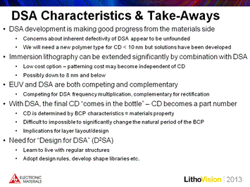
Figure 4A. A comparison of DSA vs. Spacer Quadruple patterning shows reduced process steps and fewer populations of space CDs, which helps reduce inherent overlay errors (left image). Figure 4B. Dammel summarized the DSA status and potential, as well as the need for “Design for DSA (D²SA)”.
Dammel concluded that DSA development is making very strong progress from the materials side, and said that initial concerns about inherent defectivity were unfounded. In addition, although a new polymer type will be needed for CDs < 10 nm, solutions have already been developed. Immersion lithography can also be significantly extended with DSA, providing a low cost option where patterning cost may become independent of the CD, with theoretical application down to 8 nm and beyond. He cautioned, though, that with directed self-assembly the final CD is determined by the block copolymer characteristics and that it is very difficult to change their natural periodicity. Dammel noted this will have implications for layer layout/design and necessitates “Design for DSA” (D²SA). Designers will need to learn to live with regular structures and will need to adopt design rules, and develop tools like shape libraries (figure 4B).
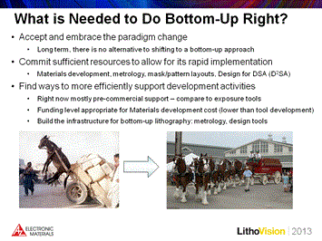
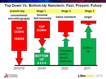
Using an analogy to the American Civil War about “Fighting yesterday’s war,” Dammel said the semiconductor industry has moved from having multiple low cost options for the next node to having no low cost option (only quadruple patterning or EUV), but the industry strategy has not kept up with this lack of technology development. He explained that, unfortunately, spending on materials is only a fraction of spending on exposure tool development and the industry needs to change its top-down lithography paradigm or the business model can’t be successful. To do bottom-up lithography successfully, the industry first needs to adjust its thinking and accept the paradigm change, then commit sufficient resources to allow for its rapid implementation through support for materials development, metrology, mask/pattern layouts, and Design for DSA. It also necessitates finding better ways to efficiently support development activities and build the necessary infrastructure for bottom-up lithography (figure 5A) including metrology and design tools. Dammel concluded his forward-thinking presentation by sharing his vision of the transition from top-down to bottom-up nanotechnology spending over the next decade and beyond (figure 5B).
